AdvancedComputer Organisation & Architecture (COA) · Lesson 9 of 10 · Updated ·
Main Memory Organisation — RAM and ROM Types, Building Memory from Chips, Address Decoding and Interleaving
Lesson 5 treated main memory as one big box that the cache talks to. In reality it is built from many small memory chips wired together. University papers and GATE regularly ask questions such as "How many 1K × 8 chips are needed for a 4K × 16 memory, and what decoder selects them?" This lesson shows how to answer them, and why memory is split into interleaved modules.
1. RAM: SRAM vs DRAM
RAM (random access memory) can be read and written, and loses its contents when power goes off (it is volatile). There are two kinds:
| SRAM (static) | DRAM (dynamic) | |
|---|---|---|
| One bit stored in | a flip-flop (about 6 transistors) | a tiny capacitor + 1 transistor |
| Refresh needed? | no — holds data while powered | yes — the charge leaks, so every row is rewritten many times a second |
| Speed | faster | slower |
| Density and cost per bit | fewer bits per chip, costly | many bits per chip, cheap |
| Used for | caches (inside the CPU) | main memory (the RAM sticks) |
This is the reason behind the memory hierarchy: you cannot afford gigabytes of SRAM, so a small SRAM cache sits in front of a large DRAM main memory.
2. ROM and its relatives
ROM (read-only memory) is non-volatile — it keeps data without power. It stores firmware, such as the code that starts a computer.
| Type | How it is written | Erased by |
|---|---|---|
| ROM (mask ROM) | at the factory | cannot be changed |
| PROM | once, by the user, with a programmer | cannot be erased |
| EPROM | by the user | ultraviolet light, whole chip |
| EEPROM | electrically | electrically, one byte at a time |
| Flash | electrically | electrically, in blocks (fast) — used in SSDs and pen drives |
3. Reading the chip notation
A chip written as N × w has N words, each w bits wide.
- A 1K × 8 chip has 1,024 locations of 8 bits — 1 KB in total.
- It needs log₂ N address lines: log₂ 1024 = 10.
- It has w data lines: 8.
So a chip of size 2ⁿ × w has n address lines and w data lines. One more input, chip select (CS), switches the chip on; when CS is off, the chip ignores the bus.
4. Building a bigger memory from chips
You can combine chips in two directions:
- Side by side (same address lines, different data lines) to make each word wider.
- Stacked in rows (different chip selects) to get more words.
Number of chips = (target words ÷ chip words) × (target width ÷ chip width).
Example. Build a 4K × 16 memory from 1K × 8 chips.
- Width: 16 ÷ 8 = 2 chips side by side in each row.
- Words: 4K ÷ 1K = 4 rows.
- Chips: 4 × 2 = 8.
- Address lines for 4K words: log₂ 4096 = 12 (A11–A0).
- Each chip uses 10 of them (A9–A0). The remaining 2 high bits (A11–A10) go into a 2-to-4 decoder, whose 4 outputs drive the chip selects of the 4 rows.
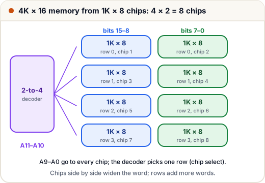
Which row holds address 2,500? Its top two bits decide: 2,500 ÷ 1,024 = 2 remainder 452, so it is row 2, location 452 within that row's chips.
The same calculation in Python, plus a larger case:
def memory_design(words, width, chip_words, chip_width):
    rows = words // chip_words          # chips stacked to get more words
    cols = width // chip_width          # chips side by side to get a wider word
    addr_lines = (words - 1).bit_length()
    chip_lines = (chip_words - 1).bit_length()
    return {
        "chips": rows * cols,
        "rows x cols": f"{rows} x {cols}",
        "address lines": addr_lines,
        "lines to each chip": chip_lines,
        "decoder": f"{addr_lines - chip_lines}-to-{rows}",
    }

K = 1024
print(memory_design(4 * K, 16, 1 * K, 8))
print(memory_design(64 * K, 16, 8 * K, 4))
{'chips': 8, 'rows x cols': '4 x 2', 'address lines': 12, 'lines to each chip': 10, 'decoder': '2-to-4'}
{'chips': 32, 'rows x cols': '8 x 4', 'address lines': 16, 'lines to each chip': 13, 'decoder': '3-to-8'}
In the second case, 64K × 16 from 8K × 4 chips: 4 chips per row, 8 rows, 32 chips, and a 3-to-8 decoder.
Quick rule for decoders: the decoder takes (total address lines − chip address lines) inputs and has one output per row.
5. Why interleave memory?
A DRAM module needs time to recover after each access (its cycle time). If consecutive addresses are all in one module, the CPU must wait for each access to finish before starting the next.
Memory interleaving spreads addresses over several independent modules (also called banks) that can work at the same time. There are two ways to split an address:
| Module number comes from | Consecutive addresses go to | |
|---|---|---|
| Low-order interleaving | the lowest bits (address mod number of modules) | different modules |
| High-order interleaving | the highest bits (address div words per module) | the same module |
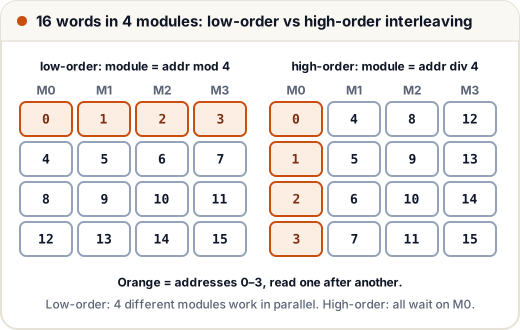
Programs and caches read consecutive addresses (a cache block, an array). With low-order interleaving, those reads hit different modules, so they overlap. High-order interleaving does not speed up sequential reads, but it lets you add memory one module at a time and keeps a faulty module's addresses in one place.
def module_and_word(addr, modules, words_per_module, low_order=True):
    if low_order:
        return addr % modules, addr // modules
    return addr // words_per_module, addr % words_per_module

for a in (0, 1, 2, 3, 13):
    lo = module_and_word(a, 4, 4, True)
    hi = module_and_word(a, 4, 4, False)
    print(f"address {a:2}: low-order -> module {lo[0]}, word {lo[1]} | high-order -> module {hi[0]}, word {hi[1]}")
address  0: low-order -> module 0, word 0 | high-order -> module 0, word 0
address  1: low-order -> module 1, word 0 | high-order -> module 0, word 1
address  2: low-order -> module 2, word 0 | high-order -> module 0, word 2
address  3: low-order -> module 3, word 0 | high-order -> module 0, word 3
address 13: low-order -> module 1, word 3 | high-order -> module 3, word 1
6. Interleaving numerical
A cache miss must bring in a block of 4 words. Each module takes 100 ns to access a word, and the bus takes 10 ns to transfer one word. Compare one module with 4-way low-order interleaving (simple model: interleaved modules start together, then send their words one after another).
access, bus, n = 100, 10, 4      # ns per module access, ns per bus transfer, words wanted

one_module = n * (access + bus)  # each read waits for the previous one
interleaved = access + n * bus   # all modules start together, then words go out one by one
print("no interleaving:", one_module, "ns")
print("4-way low-order:", interleaved, "ns")
print(f"speed-up: {one_module / interleaved:.2f}x")
no interleaving: 440 ns
4-way low-order: 140 ns
speed-up: 3.14x
- One module: 4 × (100 + 10) = 440 ns.
- Interleaved: 100 + 4 × 10 = 140 ns.
The miss penalty drops by about three times. The same idea of spreading consecutive data over independent units is why DRAM chips are divided into many banks, and why PCs with two memory sticks in matching slots (dual channel) can read faster.
Exam caution. Different textbooks use slightly different timing models (some ignore the bus time, some count a separate address-send time). Always state the model you use and follow the one given in the question.
Common mistakes
- Using log₂ of the total bytes for address lines in a word-addressed memory — use the number of words.
- Multiplying only one direction: chips = rows × columns, not just rows.
- Giving the decoder all the address lines — it gets only the bits not used inside the chip.
- Saying SRAM needs refreshing — DRAM does; SRAM does not.
- Saying high-order interleaving speeds up reading a block — it is low-order interleaving that does.
Quick recap
- SRAM: flip-flops, fast, no refresh, for caches. DRAM: capacitors, dense, needs refresh, for main memory.
- ROM family: mask ROM, PROM, EPROM (UV), EEPROM (electrical, byte), Flash (electrical, block).
- 2ⁿ × w chip: n address lines, w data lines, plus chip select.
- Chips = (words ÷ chip words) × (width ÷ chip width); decoder inputs = total address lines − chip address lines.
- Low-order interleaving: module = address mod m; consecutive words in different modules, so block reads overlap.